
Semiconductor Sealing Solutions
Ultra-Clean Sealing Systems for Vacuum, Plasma, and High-Purity Semiconductor Manufacturing
Overview
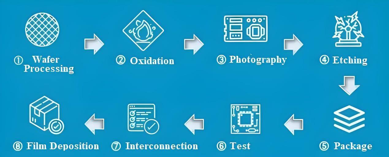 |
Semiconductor manufacturing requires ultra-clean, high-precision sealing systems to ensure process stability and high yield in applications such as wafer fabrication, etching, deposition, and vacuum processing. |
Seals are used in vacuum chambers, gas delivery systems, and plasma equipment, where even microscopic contamination, outgassing, or leakage can impact product quality and equipment performance.
These environments demand materials with ultra-low particle generation, strong chemical resistance, plasma durability, and stable performance under vacuum conditions.
Tesel Seal develops ultra-clean sealing solutions designed for high purity, reliability, and long-term performance in critical semiconductor applications.
Operating Conditions and Engineering Parameters
Vacuum Conditions
Systems operate under high or ultra-high vacuum, requiring seals to maintain tight integrity and prevent gas leakage.
Temperature Stability
Processes may involve elevated or controlled temperatures. Seals must remain dimensionally stable and resistant to thermal degradation.
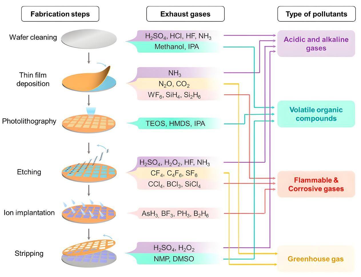
Chemical Exposure
Seals are exposed to acids, solvents, and reactive gases, requiring strong chemical resistance.
Plasma Resistance
Plasma environments can erode materials and generate particles. Seals must resist plasma-induced degradation.
Cleanroom Requirements
Ultra-low particle generation and outgassing are essential to maintain process purity and yield.
Key Challenges in Semiconductor Sealing
Particle Contamination Control
Even microscopic particles can impact wafer yield, requiring ultra-clean sealing performance.
Low Outgassing Materials
Materials must minimize outgassing under vacuum to avoid process contamination.
Plasma Resistance
Seals must resist erosion and chemical attack from ionized gases.
Chemical Compatibility
Materials must withstand aggressive chemicals without swelling or degradation.
Vacuum Integrity
Reliable sealing under vacuum conditions is essential for process stability and equipment performance.
Key Features and Performance Advantages
Sealing Technologies
At Tesel Seal, we offer a comprehensive range of sealing technologies for semiconductor applications:
Material Selection Strategy
Material selection is critical for achieving optimal sealing performance in semiconductor applications.
|
Material |
Key Benefits |
Application |
|
FFKM |
High purity, chemical resistance |
Plasma processes |
|
PTFE |
Low friction, stability |
General sealing |
|
PFA |
Chemical resistance, purity |
High purity systems |
|
FKM |
Cost-effective |
Less critical areas |
Selecting the appropriate material ensures contamination control, process stability, and long-term reliability.
Applications
Wafer Processing |
Used in etching, deposition, and cleaning systems requiring ultra-clean conditions.
|
Vacuum Chambers |
Seals maintain vacuum integrity and prevent contamination.
|
Gas Delivery Systems |
Ensure precise control and containment of process gases.
|
Chemical Handling Systems |
Require high chemical resistance and stable performance. |
Failure Analysis
Typical failure mechanisms include:
- Particle generation due to wear
- Plasma-induced material degradation
- Outgassing contamination
- Chemical attack
Understanding these mechanisms enables improved sealing design and system performance.
Performance Optimization
Optimizing sealing performance involves selecting high-purity materials, refining seal geometry, and controlling operating conditions.
Reducing contamination and extending service life are key objectives in semiconductor environments.
Buyer Guide
Key factors to consider when selecting sealing solutions:
- Cleanliness and purity requirements
- Plasma exposure conditions
- Chemical compatibility
- Vacuum level
Working with experienced engineers at Tesel Seal ensures optimal solution selection and long-term performance.
Why Choose Tesel Seal
- Expertise in ultra-clean sealing solutions for semiconductor applications
- High-purity material selection and validation
- Cleanroom-compatible manufacturing processes
- Custom-engineered solutions for critical equipment
- Engineering support throughout the product lifecycle
Custom Engineering Capabilities
At Tesel Seal, we collaborate closely with semiconductor equipment manufacturers and process engineers to develop optimized sealing solutions:
- Material selection for plasma and chemical resistance
- Precision seal design and optimization
- Cleanroom manufacturing and quality control
- Rapid prototyping and validation
Our goal is to support process stability, improve yield, and enhance long-term equipment reliability.
FAQ
What makes semiconductor seals different from industrial seals?
They require ultra-clean materials, low particle generation, and compatibility with vacuum and plasma environments.
Which materials are commonly used?
FFKM, PTFE, and PFA are widely used due to their high purity and chemical resistance.
How do sealing solutions impact wafer yield?
Sealing performance directly affects contamination control and process stability, both of which influence yield.
Do you provide custom sealing solutions?
Yes. Most semiconductor applications require tailored solutions based on specific equipment and process conditions.
Call to Action
Improve Yield. Reduce Contamination. Ensure Process Stability.Your semiconductor manufacturing process depends on ultra-clean and reliable sealing performance.
Response within 24 hours |
 |